Dr. W. Alan Doolittle


Contact Information:

Phone and Fax: 404-894-9884

Email: alan.doolittle@ece.gatech.edu

Mail:

School of Electrical and Computer Engineering

Georgia Institute of Technology

777 Atlantic Dr.

Atlanta, GA 30332-0250


Advanced Semiconductor Technology Facility


Text Box: Mission:
      The Advanced Semiconductor Technology Facility is dedicated to the advancement of semiconductor technology with the primary mission of “thinking out of the box”.  The facility’s main goal is to identify and eliminate current semiconductor limitations by combinations of established successful technology and novel, non-standard approaches.  To this end, both traditional and non-traditional tools are used in the facility.

Major Tools Include:
Traditional:
Two Riber 32 MBE systems utilizing Plasma and Ammonia sources for the growth of AlN, GaN and InN semiconductor alloys and devices.
Rare Earth Metals Varian Gen II MBE 
Full complement of characterization facilities
Novel Technologies
Photo-assisted Metal Organic MBE for mixed AlGaInN and SiC materials and devices
Chloride based Li-Metal-Oxide MBE system for Li(Nb,Ta and V ) Oxide epitaxy
High Temperature (1900° C) SiC CVD epitaxy system.


History of the Advanced Semiconductor Technology Facility

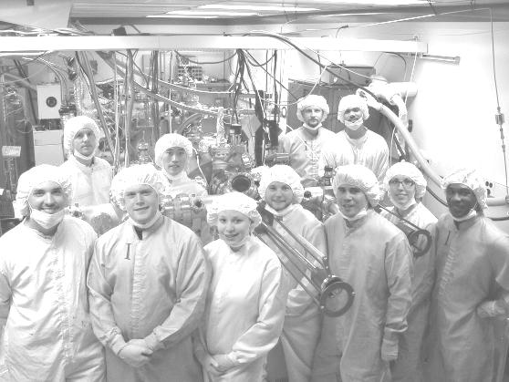
	The ASTF is housed in the Electrical and Computer Engineering, Blake R. Van Leer Building at  the Georgia Institute of Technology.  The facility occupies 1/2 of the original Microelectronics Research Center  (MiRC) originally started in 1983.  The MiRC was started with a primary vision for advancing compound semiconductor technology, a vision still replicated but also expanded today.  The ASTF facility has ~3000 square feet including ~1800 square feet of clean room space.  Currently Dr. Doolittle has primary ownership of six Georgia Tech growth systems including four commercial molecular beam epitaxy systems.
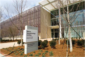
	In 1991, the Microelectronics Research Center moved into a new building which was followed in 2008 by the Nanotechnology Research Center.  The Nanotechnology Research Center (http://www.nrc.gatech.edu/) is a shared user facility consisting of two primary buildings known as the Nanotechnology Research Center (NRC) and Microelectronics Research Center (MiRC).  The NRC is a 160,000-square-foot Center augmenting capabilities in the MiRC and is the most advanced nanotechnology facility in the Southeastern United States, the first of its kind in the region, and will be one of the most sophisticated in the country. The NRC features 30,000 square feet of clean rooms critical to research and instruction in microelectronics, semi-conductors, materials, medicine, and pharmaceuticals.  The MiRC houses more than fifty multidisciplinary faculty members and 120 graduate students in a 120,000-square-footbuilding including 7,000 square feet of clean rooms.  Both the MiRC and NRC are part of The National Nanotechnology Infrastructure Network (NNIN), an integrated networked partnership of user facilities supported by the National Science Foundation that serves the needs of nanoscale science, engineering, and technology researchers.