
|
Dr. W. Alan Doolittle
|
|
Contact Information: Phone and Fax: 404-894-9884 Email: alan.doolittle@ece.gatech.edu Mail: School of Electrical and Computer Engineering Georgia Institute of Technology 777 Atlantic Dr. Atlanta, GA 30332-0250
|
|
Advanced Semiconductor Technology Facility
|
|
Characterization Tools |
|
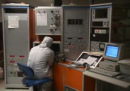
Secondary Ion Mass Spectrometry • Quantitative elemental analysis of materials • Sample composition as a function of depth • Sensitivity as high as 1 part per million
|
|
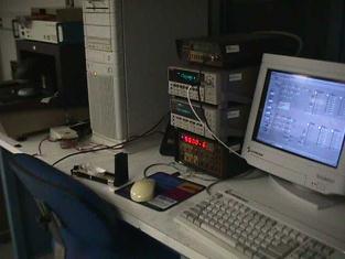
0.3 and 0-3 Tesla, temperature dependent Hall Mobility Measurement. Quantitative evaluation of mobility, carrier density and polarity.
|
|
SIMS |
|
Electron Beam Induced Current (EBIC) and Diffusion Length Mapping (DLM) |
|
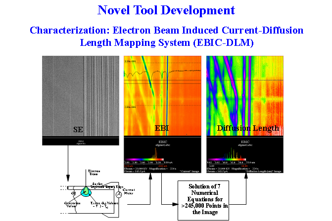
Scanning Electron Microscope (SEM) Image of an Edge Film Grown (EFG) Silicon sample
|
|
Electron Beam Induced Current (EBIC) Image(center) of the edge Film Silicon sample to the left. Note detection of electrically active defects (diagonal lines) not seen in SEM image.
|
|
Electron Beam Induced Current Diffusion Length Map (EBIC-DLM) Image of the edge Film Silicon sample to the left obtained by quantitative analysis of the EBIC image.
|
|
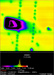
Electron Beam Induced Current (EBIC) image of decorated dislocations in SiC
|
|
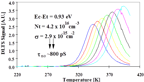
Patented High Energy Resolution DLTS system can detect very deep states in semiconductors. All important information about the defect can be determined: • Energy in the bandgap • Concentration • Capture cross-section: how strong does the defect attract electrons (or holes). • Magnetic degeneracy breakage
|
|
Patented High Energy Resolution DLTS (HER-DLTS) System
|

|
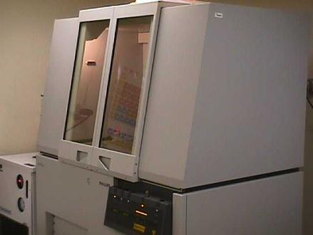
State of the Art X-ray Analysis
|
|
Field and Temperature Variable Hall Measurement |
|
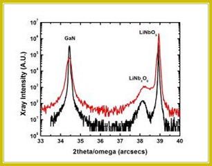
2q-w X-ray scan contrasting two samples showing reduction of undesirable substrate crystal rearrangement (LiNbO3 Þ LiNb3O8) under suitable growth conditions.
|
|
MOS Impedance and Interface Characterization |
|
Picture Missing |
|
Highlighted tools on this page (scroll down): Secondary Ion Mass Spectroscopy (SIMS) Electron Beam Induced Current (EBIC) and Diffusion Length Mapping (DLM) High Energy resolution Deep Level Transient Spectroscopy (HER-DLTS) High Resolution X-Ray Diffraction UHV STM/AFM/KPM Hall Effect Measurement MOS Impedance Characterization Electrical characterization from 40millihertz to 40 gigahertz 3 Tesla electro-magnet and 0.3 tesla permanent magnet
Partial List:
|
|
Free Access within ASTF Eight-Crystal High resolution X-Ray Diffraction Powder X-ray Diffraction High Energy Resolution-DLTS 40Hz - 110 MHz Impedance characterization (HP4294A) Capacitance -Voltage vs Temperature Current - Voltage vs Temperature Isothermal capacitance transient spectroscopy Temperature and Field dependant Hall Contactless Photoconductive Decay Electron Beam Induced Current (EBIC) EBIC-Diffusion Length Mapping (EBIC-DLM) Photoluminescence (PL) Raman Spectroscopy Radiant Technology Ferroelectric Tester Fourier Transform Infrared Spectroscopy (FTIR) Optical Reflection/Transmission Extensive equipment for DC and RF diagnostic device measurements (IV, IVT, 40 GHz Network Analyzer...)
|
|
Shared Fee Access external to ASTF Secondary Ion Mass Spectroscopy (SIMS) Atomic Force Microscopy (AFM) Electrostatic Force Microscopy (EFM) Scanning Capacitance Microscopy (SCM) Scanning Tunneling Microscopy (STM) X-ray Photoelectron Spectroscopy (XPS) Auger Spectroscopy TEM/SEM/Holographic TEM EDS/EELS
|
